Nanolayer polarizability mapping based on near-field edge fringes
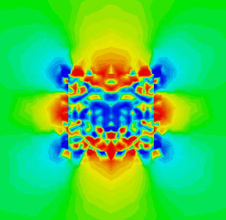
 The scattering-type scanning near-field optical microscope (s-SNOM) provides optical, chemical, and structural information about a surface and enables its imaging with nanoscale resolution. Here, we investigate nanolayers of materials with different permittivities and demonstrate an approach to identify material type based on near fields at sample edges. We have developed a theoretical method that combines full-wave numerical simulations and calculations of the s-SNOM signal of different demodulation orders. This model allows for the characterization of any shape and material structures, as well as tip characterization. Using this model, we have found that a metallic edge exhibits bright and dark fringes in near-field characterization, whereas an edge of dielectric material has no outside fringe. Similar behavior is observed in anisotropic materials with hyperbolic dispersion (boron nitride in the mid-IR range): depending on the wavelength, hBN shows either metallic or dielectric optical properties.
Publications:
[1] V.E. Babicheva, “Effective polarizability in near-field microscopy of phonon-polariton resonances,” Nanomaterials 15, 458 (2025).
[2] V. Babicheva, S. Gamage, M.I. Stockman, Y. Abate, “Near-field edge fringes at sharp material boundaries,” Opt. Express 25, 23935 (2017).
Towards understanding and control of nanoscale phase segregation in InGaN alloys
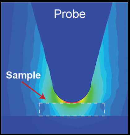
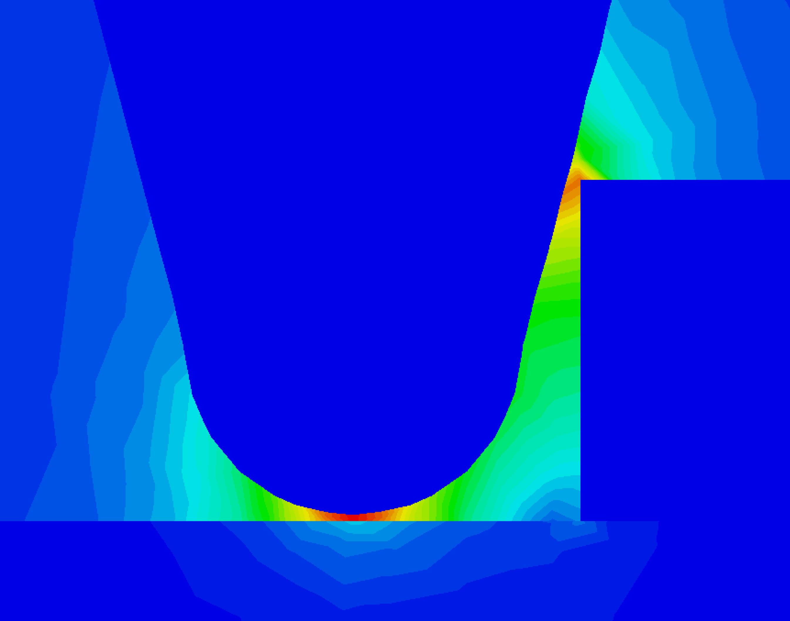
Phase separations in ternary/multinary semiconductor alloys are a major challenge that limits optical and electronic internal device efficiency. It was known early on in the advancement of growth of ternary In1-xGaxN alloys for light-emitting diodes that phase separation causes fluctuations in the band gap energy. Often, suppression of phase separation is difficult due to the different partial pressures of the constituents within the processing window, as well as an incomplete understanding of the complex thermodynamic processes during growth and a lack of detection techniques at all spatial scales relevant to device performance. Here, we have found ubiquitous local phase separation in In1-xGaxN alloys that persists on a nanoscale spatial extent by employing a high-resolution nano-imaging technique. We lithographically patterned InN/Sapphire substrates with nanolayers of In1-xGaxN down to a few atomic layers, enabling us to calibrate the near-field infrared response of the semiconductor nanolayers as a function of composition and thickness. We also developed an advanced theoretical approach that accounts for the entire geometry of the probe tip and all sample and substrate layers.
Combining experiment and theory, we identified and quantified phase separation in epitaxially grown individual nano-alloys. We found that the scale of phase separation varies widely from particle to particle, ranging from all Ga- to all In-rich regions and covering everything in between. We have found that between 20 and 25 percent of particles show any level of Ga-rich phase separation over the entire sample region, which is in qualitative agreement with the known phase diagram of In1-xGaxN system.
Publications:
[1] Y. Abate, D. Seidlitz, A. Fali, S. Gamage, V. Babicheva, V. Yakovlev, M. Stockman, R. Collazo, D. Alden, N. Dietz, “Nanoscopy of Phase Separation in InxGa1-xN Alloys,” ACS Applied Materials & Interfaces 8, 23160 (2016).
[2] Y. Abate, V.E. Babicheva, V.S. Yakovlev, and N. Dietz, “Towards Understanding and Control of Nanoscale Phase Segregation in Indium-Gallium-Nitride Alloys,” pp. 183-207, Chapter 6 in “III-Nitride Materials, Devices, and Nano-Structures,” 424 pages, Ed: Zhe Chuan Feng, World Scientific Publishing, 2017.
Nanoscopy reveals surface-metallic black phosphorus
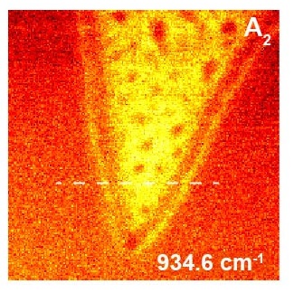
Black phosphorus is an emerging two-dimensional material with intriguing physical properties. It is highly anisotropic and highly tunable both by the number of monolayers and by surface doping. Here, we experimentally investigate and theoretically interpret near-field properties of a few-atomic-monolayer nanoflake of black phosphorus. We have discovered near-field patterns of outside bright fringes and high surface polarizability in the nanofilm of black phosphorus, consistent with its surface-metallic, plasmonic behavior at mid-infrared frequencies below 1176 cm-1. We conclude that these fringes arise from the formation of a highly polarizable layer at the black phosphorus surface. This layer has a thickness of ~1 nm and exhibits plasmonic behavior. Surface plasmonic behavior has been found for 10–40 nm thickness of black phosphorus, but is absent for 4 nm thickness. This discovery opens up a new field of research and potential applications in nanoelectronics, plasmonics, and optoelectronics.
Publications:
[1] Y. Abate, S. Gamage, L. Zhen, S.B. Cronin, H. Wang, V. Babicheva, M.H. Javani, M.I. Stockman, “Nanoscopy reveals surface-metallic black phosphorus,” Light: Science & Applications 5, e16162 (2016).